Impurities
"RCA Transistor Manuel"
TECHNICAL SERIES SC–13
Copyright 1967 by Radio Corporation of America
Semiconductor devices are small but versatile units that can perform an amazing variety of control functions in electronic equipment. Like other electron devices, they have the ability to control almost instantly the movement of charges of electricity. They are used as rectifiers, detectors, amplifiers, oscillators, electronic switches, mixers, and modulators.
In addition, semiconductor devices have many important advantages over other types of electron devices. They are very small and light in weight ( some are less than an inch long and weigh just a fraction of an ounce ). They have no filaments or heaters, and therefore require no heating power or warm-up time. They consume very little power. They are solid in construction, extremely rugged, free from microphonics, and can be made impervious to many severe environmental conditions. The circuits required for their operation are usually simple.
Unlike other electron devices, which depend for their functioning on the flow of electric charges through a vacuum or a gas, semiconductor devices make use of the flow of current in a solid. In general, all materials may be classified in three major categories — conductors, semiconductors, and insulators — depending upon their ability to conduct an electric current. As the name indicates, a semiconductor material has poorer conductivity than a conductor, but better conductivity than an insulator.
The materials most often used in semiconductor devices are germanium and silicon. Germanium has higher electrical conductivity ( less resistance to current flow ) than silicon, and is used in most low– and medium–power diodes and transistors. Silicon is more suitable for high–power devices than germanium. One reason is that it can be used at much higher temperatures. A relatively new material which combines the principal desirable features of both germanium and silicon is gallium arsenide. When further experience with this material has been obtained, it is expected to find much wider use in semiconductor devices.
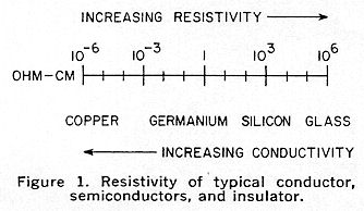
The ability of a material to conduct current ( conductivity ) is directly proportional to the number of free ( loosely held ) electrons in the material. Good conductors, such as silver, copper, and aluminum, have large numbers of free electrons; their resistivities are of the order of a few millionths of an ohm-centimeter. Insulators such as glass, rubber, and mica, which have very few loosely held electrons, have resistivities as high as several million ohm-centimeters.
Semiconductor materials lie in the range between these two extremes, as shown in Fig. 1. Pure germanium has a resistivity of 60 ohm–centimeters. Pure silicon has a considerably higher resistivity, in the order of 60,000 obm-centimeters. As used in semiconductor devices, however, these materials contain carefully controlled amounts of certain impurities which reduce their resistivity to about 2 ohm–centimeters at room temperature ( this resistivity decreases rapidly as the temperature rises ).
Impurities
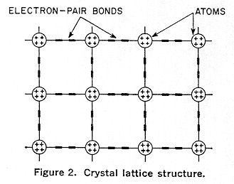
Carefully prepared semiconductor materials have a crystal structure. In this type of structure, which is called a lattice, the outer or valence electrons of individual atoms are tightly bound to the electrons of adjacent atoms in electron–pair bonds, as shown in Fig. 2. Because such a structure has no loosely held electrons, semiconductor materials are poor conductors under normal conditions. In order to separate the electron pair bonds and provide free electrons for electrical conduction, it would be necessary to apply high temperatures or strong electric fields.
Another way to alter the lattice structure and thereby obtain free electrons, however, is to add small amounts of other elements having a different atomic structure. By the addition of almost infinitesimal amounts of such other elements, called "impurities", the basic electrical properties of pure semiconductor materials can be modified and controlled. The ratio of impurity to the semiconductor material is usually extremely small, in the order of one part in ten million. ( 0.1 ppm )
When the impurity elements are added to the semiconductor material, impurity atoms take the place of semiconductor atoms in the lattice structure. If the impurity atoms added have the same number of valence electrons as the atoms of the original semiconductor material, they fit neatly into the lattice, forming the required number of electron–pair bonds with semiconductor atoms. In this case, the electrical properties of the material are essentially unchanged.
When the impurity atom has one more valence electron than the semiconductor atom, however, this extra electron cannot form an electron pair bond because no adjacent valence electron is available. The excess electron is then held very loosely by the atom, as shown in Fig. 3, and requires only slight excitation to break away. Consequently, the presence of such excess electrons makes the material a better conductor, i.e., its resistance to current flow is reduced.
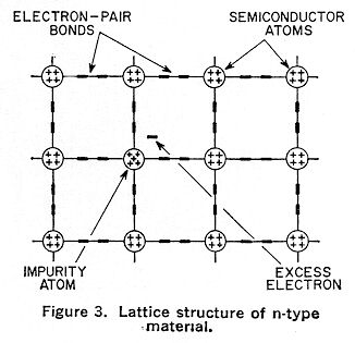
Impurity elements which are added to germanium and silicon crystals to provide excess electrons include arsenic and antimony. When these elements are introduced, the resulting material is called n–type because the excess free electrons have a negative charge. ( It should be noted, however, that the negative charge of the electrons is balanced by an equivalent positive charge in the center of the impurity atoms. Therefore, the net electrical charge of the semiconductor material is not changed. )
A different effect is produced when an impurity atom having one less valence electron than the semiconductor atom is substituted in the lattice structure. Although all the valence electrons of the impurity atom form electron–pair bonds with electrons of neighboring semiconductor atoms, one of the bonds in the lattice structure cannot be completed because the impurity atom lacks the final valence electron. As a result, a vacancy or "hole" exists in the lattice, as shown in Fig. 4. An electron from an adjacent electron–pair bond may then absorb enough energy to break its bond and move through the lattice to fill the hole. As in the case of excess electrons, the presence of "holes" encourages the flow of electrons in the semiconductor material; consequently, the conductivity is increased and the resistivity is reduced.
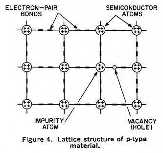
The vacancy or hole in the crystal structure is considered to have a positive electrical charge because it represents the absence of an electron. ( Again, however, the net charge of the crystal is unchanged. ) Semiconductor material which contains these "holes" or positive charges is called p–type material. p–type materials are formed by the addition of aluminum, gallium, or indium.
Although the difference in the chemical composition of n–type and p–type materials is slight, the differences in the electrical characteristics of the two types are substantial, and are very important in the operation of semiconductor devices.
When n–type and p–type materials are joined together, as shown in Fig. 5, an unusual but very important phenomenon occurs at the interface where the two materials meet ( called "the p-n junction" ). An interaction takes place between the two types of material at the junction as a result of the holes in one material and the excess electrons in the other.
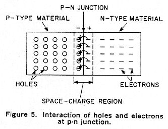
When a p–n junction is formed, some of the free electrons from the n-type material diffuse across the junction and recombine with holes in the lattice structure of the p–type material; similarly, some of the holes in the p–type material diffuse across the junction and recombine with free electrons in the lattice structure of the n–type material. This interaction or diffusion is brought into equilibrium by a small space–charge region ( sometimes called the transition region or depletion layer ). The p–type material thus acquires a slight negative charge and the n–type material acquires a slight positive charge.
Thermal energy causes charge carriers ( electrons and holes ) to diffuse from one side of the p–n junction to the other side; this flow of charge carriers is called diffusion current. As a result of the diffusion process, however, a potential gradient builds up across the space–charge region. This potential gradient can be represented, as shown in Fig. 6, by an imaginary battery connected across the p–n junction. ( The battery symbol is used merely to illustrate internal effects; the potential it represents is not directly measurable. )
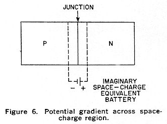
The potential gradient causes a flow of charge carriers, referred to as drift current, in the opposite direction to the diffusion current. Under equilibrium conditions, the diffusion current is exactly balanced by the drift current so that the net current across the p–n junction is zero. In other words, when no external current or voltage is applied to the p–n junction, the potential gradient forms an energy barrier that prevents further diffusion of charge carriers across the junction. In effect, electrons from the n–type material that tend to diffuse across the junction are repelled by the slight negative charge induced in the p-type material by the potential gradient, and holes from the p–type material are repelled by the slight positive charge induced in the n–type material. The potential gradient ( or energy barrier, as it is sometimes called ), therefore, prevents total interaction between the two types of materials, and thus preserves the differences in their characteristics.
When an external battery is connected across a p–n junction, the amount of current flow is determined by the polarity of the applied voltage and its effect on the space–charge region. In. Fig. 7a, the positive terminal of the battery is connected to the n–type material and the negative terminal to the p–type material.
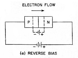
In this arrangement, the free electrons in the n–type material are attracted toward the positive terminal of the battery and away from the junction. At the same time, holes from the p–type material are attracted toward, the negative terminal of the battery and away from the junction. As a result, the space–charge region at the junction becomes effectively wider, and the potential gradient increases until it approaches the potential of the external battery. Current flow is then extremely small because no voltage difference ( electric field ) exists across either the p–type or the n–type region. Under these conditions, the p–n junction is said to be reverse–biased.
In Fig. 7b, the positive terminal of the external battery is connected to the p–type material and the negative terminal to the n–type material.
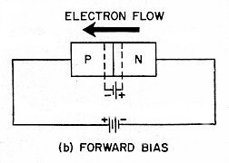
In this arrangement, electrons in the p–type material near the positive terminal of the battery break their electron–pair bonds and enter the battery, creating new holes. At the same time, electrons from the negative terminal of the battery enter the n–type material and diffuse toward the junction. As a result, the space charge region becomes effectively narrower, and the energy barrier decreases to an insignificant value. Excess electrons from the n–type material can then penetrate the space charge region, flow across the junction, and move by way of the holes in the p–type material toward the positive terminal of the battery. This electron flow continues as long as the external voltage is applied. Under these conditions, the junction is said to be forward–biased.
The generalized voltage–current characteristic for a p–n junction in Fig. 8 shows both the reverse–bias and forward–bias regions.
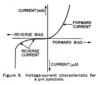
In the forward–bias region, current rises rapidly as the voltage is increased and is quite high. Current in the reverse–bias region is usually much lower. Excessive voltage ( bias ) in either direction should be avoided in normal applications because excessive currents and the resulting high temperatures may permanently damage the semiconductor device.
Fig. 7 shows that a p–n junction biased in the reverse direction is equivalent to a high–resistance element ( low current for a given applied voltage ), while a junction biased in the forward direction is equivalent to a low–resistance element ( high current for a given applied voltage ). Because the power developed by a given current is greater in a high–resistance element than in a low–resistance element ( P=I2R ), power gain can be obtained in a structure containing two such resistance elements if the current flow is not materially reduced. A device containing two p–n junctions biased in opposite directions can operate in this fashion.
Such a two–junction device is shown in Fig. 9.
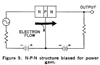
The thick end layers are made of the same type of material ( n–type in this case ), and are separated by a very thin layer of the opposite type of material ( p–type in the device shown ). By means of the external batteries, the left–hand ( p–n ) junction is biased in the forward direction to provide a low–resistance input circuit, and the right–hand ( p–n ) junction is biased in the reverse direction to provide a high–resistance output circuit. ...
I have many trade magazines and component manuals, with technical discussions presented by the people who developed and marketed much of today's technology. Who better to describe the workings of the world around us to our children, who have desperate need of this knowledge ? We have already discovered all the science we need to solve ALL our problems. We ALL just need to learn a little of it. Somehow, this funny little [ 100 meg ] web site has become a center for the presentation of this information. I just wanted a private little corner of the Internet to keep my research notes and material, so I could get at it during my travels. All of a sudden, I started getting a flood of e-mail. Much of it coming from people with "Doctor" in their names, many wanting to help by submitting material. In the name of Education, this web site doesn't post commercial ads or charge fees. It has no tangible source of income. Donations are needed to help keep this web site a viable educational tool. Donations can be sent to ...
Tommy Cichanowski
Thanks for reading this, and please help.
Donors will be sent a copy of this web site on CD.
|
" Control of Colloid Stability through Zeta Potential "
Dr. T.C. McDaniel — "Using Zeta Potential as a Healing Tool"
The Wonderful World of Advanced Materials
Using Hydroponics to Understand the Earth's Life Processes
Tommy's History Of Western Technology
by Thomas M. Riddick ( Understanding "Valance Possibilities" )
On the Atomic Level